
The Streamroller project focuses on design on system of loop accelerators, primarily for media and wireless applications. A loop accelerator implements a critical loop from an application with far greater performance and efficiency than would be possible with a programmable implementation. Multiple loop accelerators are strung together in a hardware pipeline to meet the overall throughput requirements for a whole application while minimizing hardware costs.
Designing Systems of Accelerators
The Streamroller design system takes a sequential C program and automatically designs a system of loop accelerator for it.
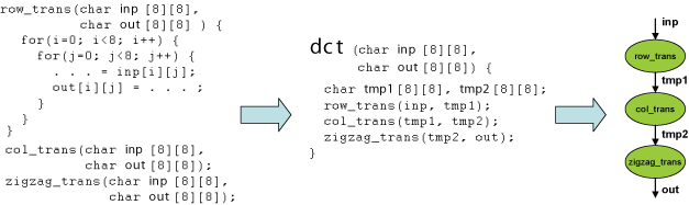
The input C program is stylized, and is divided into kernel specification and system specification. The above picture shows an example of an input application. Kernel specification describes a single loop, whereas system specification describes the communication pattern between loops. From the system specification, a data structure called the "loop graph" is derived, which is used in the later phases of Streamroller design system.
Multifunction Loop Accelerators
Once the system of accelerators is designed, the task remains to design the accelerators themselves. The goal is to achieve high degrees of performance, area efficiency, and energy efficiency by creating specialized hardware for a given loop or set of loops. The loop is software pipelined to expose more parallelism, and the loop accelerator datapath is designed to perform the required computations and data transfers while achieving a desired initiation interval, or II.
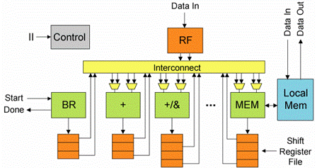
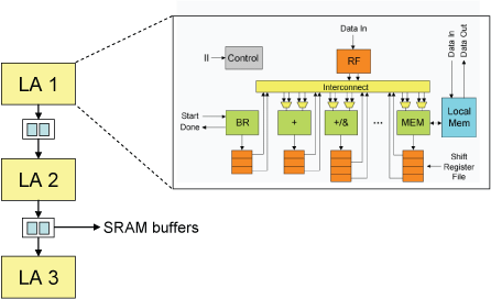
The above figure shows our loop accelerator schema. It consists of function units, shift register files (SRFs), and local memories, connected to each other with an efficient interconnection scheme. The use of distributed, few-ported structures such as SRFs and local memories allow scaling of the loop accelerator to achieve high performance while avoiding high wire delays and energy consumption. The numbers and types of all of these datapath elements are intelligently determined from the characteristics of the application.
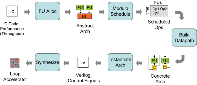
A compiler-centric approach is used to analyze the loop and synthesize the hardware. The flow diagram is shown above. First, an abstract VLIW architecture is created which is parameterized by the number of FUs and their capabilities. Next, the loop is modulo scheduled to this abstract architecture. Then, the accelerator datapath is determined from the producer-consumer relationships in the schedule. This includes setting the widths of the FUs and the widths and depths of the SRFs, and connecting specific SRF entries with the appropriate FU inputs. Finally, a Verilog realization of the accelerator is generated and synthesized.
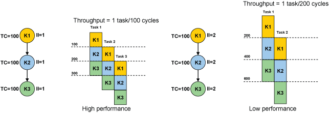
To produce efficient designs, it's necessary to leverage hardware sharing to reduce cost. This can take the form of intra-loop sharing, which focuses on operations within a loop, and inter-loop sharing, in which multiple loops are mapped onto the same hardware accelerator. To improve intra-loop hardware sharing, it is necessary to have a cost-aware modulo scheduler since the datapath is derived from the schedule. The scheduler should arrange operations such that FUs, SRFs, and wires are reused across operations where possible (note this only applies for designs where II > 1). To improve inter-loop hardware sharing, all of the loops should be intelligently mapped to the same datapath such that maximal reuse occurs and the final datapath cost can be reduced. Please refer to publications about cost sensitive scheduling and multifunction accelerator design (listed below) for details.
Architecture Design Framework
The architecture design framework is an important part of the synthesis system. In the figure below, the components in the blue box make up the architecture design framework. The hardware compiler generates a high level architecture specification (or archspec) based on the application and a parallelism specification. From this archspec, various phases of architecture synthesis must be performed which will accomplish the following tasks:
- Generate a low level architecture description with detailed information about the implementation of functionality and connectivity within the architecture.
- Estimate the hardware cost of the architecture.
- Generate HDL for the architecture.
- Generate a machine description which will be used by the retargetable compiler to compile the application for the architecture.
- Generate an architecture simulator to verify the design and provide performance and power estimates.
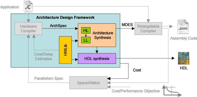
Key to the architecture design framework is the internal description of the architecture. In our system, a multi-level architecture description is used. This gives the advantages of both high and low level representations. A high level representation (labeled HL in the above figure) is generated from the hardware compiler's archspec. This includes information such as the number and types of function units and register files, and high level connectivity information, much like a hardware block diagram. This representation is then lowered during the Architecture Synthesis phase to the low level representation (labeled LL). This includes details such as specific port connections, multiplexers, and selection of macrocells. Cost estimates and HDL are generated from the low level representation.
To generate cost estimates and HDL for a given architecture, a hardware library (labeled HWLib in the system flow diagram above) is used. This library contains parameterized area, power, and delay estimates for the components in the processor, including the register files, function units, and multiplexers. From the low level architecture description and this hardware library, a cost estimate can be obtained for the processor. The hardware library also contains a structural verilog implementation for each of the architecture components. By using these components as building blocks, synthesizable HDL can be generated for the entire processor.
Generation of a compiler-oriented machine description consists of extracting resources, resource usage patterns, and physical input-output formats from the architecture description. The compiler will use the resources to model the concurrency available in the machine; thus, resources are components such as function units, register file ports, and buses. These resources and their usage patterns are obtained from the architecture description. Input-output formats are determined from the connections between function units and register files in the machine.
Relevant Publications
Page last modified January 22, 2016.